


Investigation of mounting techniques for SMD capacitors1 Aprilie 2020
Introduction
Capacitors, they store charge with the price of voltage between two plates separated by a dielectric. The main parameter that describes them is the capacitance and that is all we would like to find inside a capacitor, but how nothing in perfect in life, a small series (or parallel, depends of what model you choose to use) inductance and resistance will always be present in a real capacitor. Why are these parts needed? of course for many reasons in lots of applications but in the high frequency domain mainly for decoupling.
In this article I used a simple series RLC model to describe a capacitor, where the C describes the desired effect of the component, the one of storing electric charge and the R and L describe the parasitic ones. Since we are discussing about a series RLC circuit, our minds immediately goes to a minimum peak in the impedance of this circuit at the self-resonating frequency (abbreviated SRF). This frequency which only depends of the total L and C of the RLC circuit is the turning point where our real capacitor changes its behavior from a capcitive one to an inductive one so estimating this value is essential.
Needless to say that manufacturers give highly detailed data sheets with all these three RLC parameters, their variations and many more included. However, between what a manufacturer sells and what we use in our system stands the interconnect: the circuit board that connects the electronic part to the rest of the circuits. If the equivalent series resistance (usually abbreviated ESR) is not highly influenced by the mounting technique, the equivalent series inductance (usually abbreviated ESL) is dramatically increased by the loop inductance of the mounting VIAs and traces used to connect the part to the power planes.
The mounting inductance, a quantity that adds to the ESL of the component, comes from the VIAs and traces almost mandatory to use for connecting a capacitor to the VCC and GND planes usually buried deep into the core of the circuit board. As seen in Figure 1, the two VIAs are crossed by opposite currents, one into the capacitor and one out of the capacitor. In this article I investigated how different mounting techniques of these capacitors (with one or more than one VIA pairs) influence this mounting inductance. I presented in the end the results obtained from three different methods: one analytical approach and two simulation setups using Ansys HFSS 3D Layout. The error with which the analytical approach can predict the mounting inductance is also discussed along with its possible causes.
Final conclusions are drawn about the best mounting technique (also called mounting style in this article) to be used in a circuit board and what further issues rises choosing one over another.
 Figure 1: Current loop under a capacitor connected through VIAs
ECAD board design
Before we start, let me briefly recap how the series RLC circuit we are going to use to describe the behavior of our real capacitor works and what are its main figures of interest. Having two different reactive components in series will give rise to two opposite behaviors of the series impedance of this circuit: one dropping with frequency characteristic to the C in our circuit and one rising with frequency characteristic to the L in our circuit. The point where this shift takes place is already mentioned SRF and can be calculated with Equation 1, where if used in its second form the L and C values must be in nH respectively nF to give the proper result in MHz. The final figure of interest for this discussion is the ESR which describes the lowest value that the impedance of the circuit takes when the frequency reaches the SRF value.
 Equation 1: SRF Frequency
You can see in Figure 2 the impedance plot of the series circuit I used to describe all the capacitors from this article. With a capacitance of 100nF, ESL of 0.4nH and ESR of 0.01W we expect a SRF of 25.15MHz and a lowest possible value of the impedance of 0.01W. These exact results are revealed now by simulation. However, in the following examples including the interconnect (the ECAD board with its power planes and VIAs) and simulated using Ansys HFSS 3D Layout you shall see that the SRF is considerably smaller than this value since to the ESL the mounting inductance will unfortunately add up.
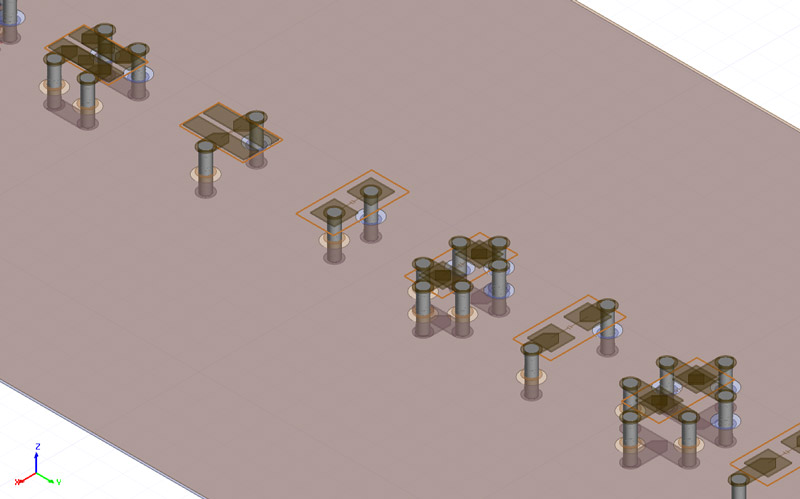
Moving to today’s topic I start by presenting the ECAD structure designed in order to investigate different mounting techniques for decoupling capacitors: a very simple 8 layers 1 by 2 inches circuit board with a stack-up presented in Figure 3 where 11 capacitors (Ref Designator C1 to C11) were placed in different ways called "Mounting style 1" to "Mounting style 11". A top view of the board with all these 11 mounting styles is provided in Figure 4.
 Figure 2: Series RLC circuit impedance plot
Capacitors C1 to C8 have a 0603 (1608 metric) footprint while C9 to C11 are 0306 (0816 metric) reverse aspect ratio which can significantly reduce mounting inductance. All the VIA holes in the design have 16MIL diameter (abbreviated D) and a VIA pad of 24MIL. The traces used to connect the capacitor to the VIA have the width of 24MIL and only the traces used for C1 have a width of 5MIL. The via spacing (abbreviated S) varies from 178MIL in the case of C1 and goes down to 57MIL for C8 (mounting style VIA-in-pad).
The mounting inductance of a capacitor comes from the current loop described in Figure 1, where each VIA behaves as a small (on not so small) inductor and therefore has a self inductance which we could call L1 and L2 and also a mutual inductance between one and another, called L12 and 21. Since L12 and L21 are equal we call this mutual inductance simply LM. With these figures set in place, we can now give a formula for the loop inductance of two inductors crossed by opposite currents in Equation 2.
 Equation 2: Loop Inductance - opposite current flows
 Figure 3: Test circuit board stack-up
On the topic of mutual inductance there is more to discuss since it is a powerful tool in the high frequency design. Mutual inductance is all about the magnetic filed lines surrounding one inductor but caused by the current crossing another closed inductor. Since the inductors have opposite currents and field lines, the mutual inductance is subtracted from the total. Our intuition combined with Equation 2 in mind gives us the first knob we must adjust to lower loop inductance: setting the opposite current VIAs as close as possible to benefit from the help of the mutual inductance. The exact opposite action should be taken when having VIAs crossed by current in the same way how is the case of the three VIAs to GND from C3. Setting VIAs crossed by current in the same way as far as possible is the right action to take since the mutual inductance now becomes our enemy by adding to the loop inductance as you can see in Equation 3.
 Equation 3: Loop Inductance - same current flows
One important contribution to the mounting inductance besides the loop is the traces inductance. We expect a higher inductance in the case of a narrow trace such as in the example of C1 than in the case of a wide trace such as the C2. In fact, the difference in mounting indctance from C1 to C2 will be totally caused by the narrow track used in the case of C1.
Now that we have all the geometrical data listed we can calibrate our intuition further more and discuss what result should we expect from the simulations. First of all reducing the spacing between VIAs crossed by opposite currents should also reduce the mounting inductance. This is why we would expect the mounting style No. 8 (via-in-pad) to have a lower inductance than mounting style No.6. Furthermore, adding more VIA pairs in parallel should reduce the mounting inductance from only one VIA pair how should be the case of C5 with regard to C4.
We can also predict the result of our simulation with analytical approaches. One approach would be to use an analytical approximation to estimate the self and mutual inductance for each VIA in a VIA pair and then with the above equations to calculate the loop inductance. However, I opted for a simpler analytical approach using Equation 4 for the loop inductance of a VIA pair given by Eric Bogatin in [1].
 Figure 4: TOP view of the board
 Equation 4: Loop Inductance analytical approximation
The result is obtained in the units of m0 and is a linear loop inductance. In order to scale it up for a particular geometry, you must mutiply it with the height of the VIA pair which in all my examples was 33MIL as you can notice from Figure 1.
Loop inductance extracted from S11
Discussing all the aspects regarding the analytical approach we now move to the simulation setup of this investigation. In this section I will present how the mounting inductance of one pair of VIAs is extracted using Ansys HFSS 3D Layout. All the capacitors models are disabled in this stage of simulation since we are only interested by the mounting inductance of the interconnect. Very important to mention is that this setup will give us the mounting inductance which includes the loop and tracks inductance.
I followed a procedure used usually in a one port VNA measurement of a Device Under Test (abbreviated DUT), in our case the DUT being the VIAs loop. I shorted the VIA structure with a 0Ω Port2 at the bottom of the board to create the desired current loop and I defined one more 50Ω Port1 at the top of the structure as can be seen in Figure 5. In this way, Port1 has a scattering parameter S11 as defined in Equation 5 which can be rearranged with a little algebra in the form from Equation 6, where ZDUT is nothing more than the impedance of our loop. Finally we can approximate al low frequency our structure with a simple lumped inductor, whose value can be extracted in the way described by Equation 7.
 Equation 5: S11 formula from voltage reflection coefficient
 Equation 6: DUT impedance from S11
 Equation 7: Inductance from DUT impedance
 Figure 5a: Port setup for one VIA pair
 Figure 5b: Port setup for multiple VIA pairs
 Figure 6: Loop inductance for Mounting style No. 3
The L plot can be seen for the Mounting style No. 3 in Figure 6 where you can also observe that this approximation of our structure with a simple lumped inductor is valid only up to 0.1GHz. After this point a distributed model might be needed. However, this is not a limitation for us since I extracted the loop inductance at a small frequency around 5MHz. Lastly on this topic I must mention that the simulation provided the loop for the whole 59MIL height loop but our effective loop is only 33MIL as described in Figure 1, reason why I scaled the result for our height of interest.
Loop inductance extracted from SRF
Another approach can be used to extract the mounting inductance for each mounting style in this project. This is based on determined through simulation the SRF of the RLC circuit and extracting the total inductance from Equation 1. If the capacitance is considered to remain constant to 100nF since contribution from the VCC and GND plane capacitance is very small we can easily obtain the total inductance of the real capacitor, from which we subtract the ESL to determine the mounting inductance.
You can see the simulation setup in Figure 7 where at each side of the board 50W Ports were applied between the VCC and GND planes. The transfer impedance between these two ports is exactly our capacitor’s impedance since only one capacitor was enabled from the HFSS 3D Layout components menu at once. I performed a frequency sweep only in the frequency interval of interest from 5MHz to 30MHz where I expected all the 11 SRF points to reside. Moreover, a very important step in simulating high Q resonators structures is to explicitly set the solver to solve the structure for a frequency close to the estimated resonance since otherwise you only rely on the interpolation algorithm, which might miss or over or under estimate the SRF point.
 Figure 7: Port setup for SRF simulation
You can see the simulation result in Figure 8, a plot over frequency for the transfer impedance of our structure when only C3 was activated.
 Figure 8: Series RLC SRF point Mounting style No. 3
Results
You can now see in Figure 9 all the results of this investigation listed for all of the 11 mounting styles. The chosen RLC model for all the capacitors was the same for all types and values of ESR, ESL and C are listed in the 3rd to 5th column only for consistency. The following columns are discussed in the following paragraphs.
Diameter of the VIA - DVIA and spacing between VIAs - S are geometrical aspects of our structure. These two figures along with the mounting style of the capacitor are the main knobs you can adjust to get a lower mounting inductance. The spacing for one VIA pair mounting styles is exactly the center-to-center spacing between the two VIAs of the pair while fore more than one VIA pairs styles the spacing in an average between the smallest and largest value of spacing. This gives rise to a series of errors discussed in the following section of this article.
The analytical loop inductance - Lloop-an was calculated using Equation 4 with the result scaled to 33MIL, the height of our VIA loop. For the more than one VIA pairs structures the result given of Equation 4 and scaled to 33MIL was further divided by the number of VIA pairs since these structures are in a parallel configuration which lowers the inductance. In the 8th column of our table the final result after division is noted.
The analytical inductance of the traces - Ltraces-an used to connect the capacitor’s pads to the VIAs are only calculated for mounting styles No.1 to No. 5 and considered to be null for the other ones. Using simple analytical approximation tools knowing the trace width (5MIL or 24MIL) and height over the GND plane (33MIL) the linear inductance of the tracks was obtained which was finally scaled to the length of the trace. Once again, in the 9th column of the table only the final results are noted.
The analytical mounting inductance - Lmount-an was obtained by adding the analytical loop inductance - Lloop-an with the analytical inductance of the traces - Ltraces-an.
The simulated mounting inductance - Lmount-sym is obtained from the first setup simulation described in this article. Bear in mind that the values provided by HFSS 3D Layout are for a complete 59MIL loop height so the ones in our table are scaled to only 33MIL height.
The SRF values were obtained for each mounting style by the second simulation setup described above. I should once again mention that before each SRF simulation I used the Lmount-sym which I added to the ESL to estimate what the RLC circuit resonance frequency would be to constrain the simulator to also solve the structure at that precise frequency.
Results of mounting inductance from SRF simulation Lmount-SRF were determined using the SRF simulated points and Equation 1. To obtain the mounting inductance the ESL was subtracted from the obtained values.
 Figure 9: Simulation and analytical results
You can observe in Figure 10 the mounting inductance for each mounting style investigated in this article. The graph from Figure 10 includes the data from Lmount-sym the reason being discussed in the following section.
Errors
I present now the main sources of error for the simulations and for the analytical approach. By far the highest source of error is the approximation I made for the more than one VIA pairs mounting structures. While dividing by the number of VIAs the result obtained from Equation 4 is a fair assumption, I totally neglect the fact that coupling might exist between VIAs with the same current flow. This type of coupling is the one that adds to the total loop inductance according to Equation 3 and that is why the analytical approach provided considerably lower results than the simulation setup Lmount-sym in the case of mounting style No. 3,5,7,10 and 11.
 Figure 10: Mounting inductance for different mounting styles
Secondly, Ansys HFSS 3D Layout calculates a slightly higher Lmount-sym mounting inductance than the analytical approach for the mounting styles with only one VIA pair because it also takes into account non-uniform current distribution entering and leaving the VIA pair and some non-uniform magnetic fields at the top and bottom of the VIA pair.
Last but not least, the mounting inductance simulated using the SRF techniques is slightly higher than the one simulated using just the VIAs loop because the SRF setup has the ports at the margins of the VCC and GND planes, which also adds some inductance from the planes to the mounting inductance that we were trying to obtain. This is the reason why I considered the best simulation setup to be the first one.
You can observe in Figure 11 the error of the analytical approach with regard to the values of Lmount-sym. As expected, where more than one VIA pair is present this analytical approach gives a higher than 20% error rate.
Conclusion
In the final section of this article I arranged the mounting styles investigated in order of the mounting inductance from the smallest to the largest. This arrangement is present in Figure 12. Choosing one over another is one of the classic trade-offs HF Engineers must do. Of course the via-in-pad would give the lowest mounting inductance with the same classic 0603 footprint and would also save space on the board but it would also rise problems in the assembly stages for the PCB. And by far the reverse aspect ratio 0306 with 4 pair of VIAs provides the best mounting inductance but this 0306 capacitor might come with a higher price per unit.
 Figure 11: Error of analytical formula
 Figure 12: Mounting styles sorted by inductance
I have not mentioned so far the total inductance of the capacitor, the mounting inductance added to the ESL which is basically what the IC decoupled by that capacitor must live with. I present these numbers in the final graph of this article in Figure 13. You can observe here the contribution to the total inductance of the mounting style and the traces. Now is by far best seen why the total inductance of a capacitor is not only a responsibility of the parts manufacturer but also a result of the layout process a HF Engineer has to perform.
 Figure 13: Total inductance of the capacitor