High Frequency Simulation and Verification Course1 Septembrie 2020
Introduction
In the autumn of 2019 we started a High Frequency Simulation and Verification Course using ANSYS products at the Faculty of Electronics, Bucharest. It consisted of 3 hours laboratory sessions taking place every 2 weeks. The course reunited undergraduate, master and even PhD students since participation was optional.
I structured the course subjects in 5 chapters as follows: Transmission Lines Fundamentals, Transmission Lines and Reflections, S-Parameters for Signal Integrity Applications, Lossy Transmission Lines and Cross Talk in Transmission Lines. Every topic included a small theoretical part followed by practical exercises using ANSYS HFSS or Siwave. The virtual prototyping applications were reduced in terms of the required processing power, each taking roughly less than 10 minutes to simulate on a standard personal computer.
In order to better present some high-frequency effects, I also developed a PCB hardware platform called LABSKEW based on Stephen Thierauf’s book, Introduction to Signal Integrity: A Laboratory Manual. The platform had various components that could be easily inserted into the circuit with jumpers and a 10-meters long CAT5e cable was used as transmission line. Participants of the course also investigated with an oscilloscope near and far-end signals with different termination techniques. Other concept that were investigated using the LABSKEW hardware platform included cross talk, transmission line delay, reflections and characteristic impedance.
Methodology
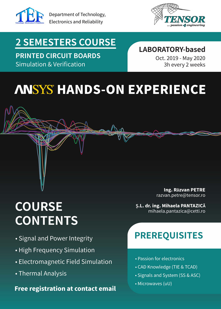 Figure 1: Simulation and Verification Course - poster promoted in the University and on
social media channels including prerequisites and course contents.
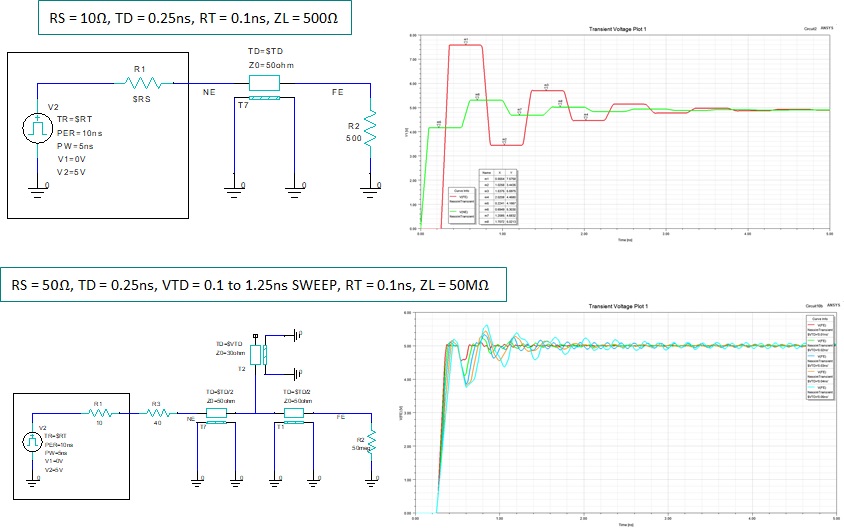 Figure 2: Transmission line source series termination investigation or VIA stub modeling by
simulation in ANSYS Electronics Desktop. Other simulation exercises also include parasitic
extraction from existing ECAD designs.
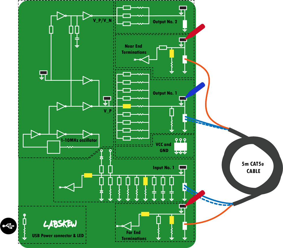 Figure 3: LABSKEW - PCB hardware platform custom-made for the Simulation and Verification
Course, transmission line is a long (5 or 10m) CAT5e cable, different source series of
far end terminations are available with jumper connectors.
Figure 3: LABSKEW - PCB hardware platform custom-made for the Simulation and Verification
Course, transmission line is a long (5 or 10m) CAT5e cable, different source series of
far end terminations are available with jumper connectors.Hardware Design
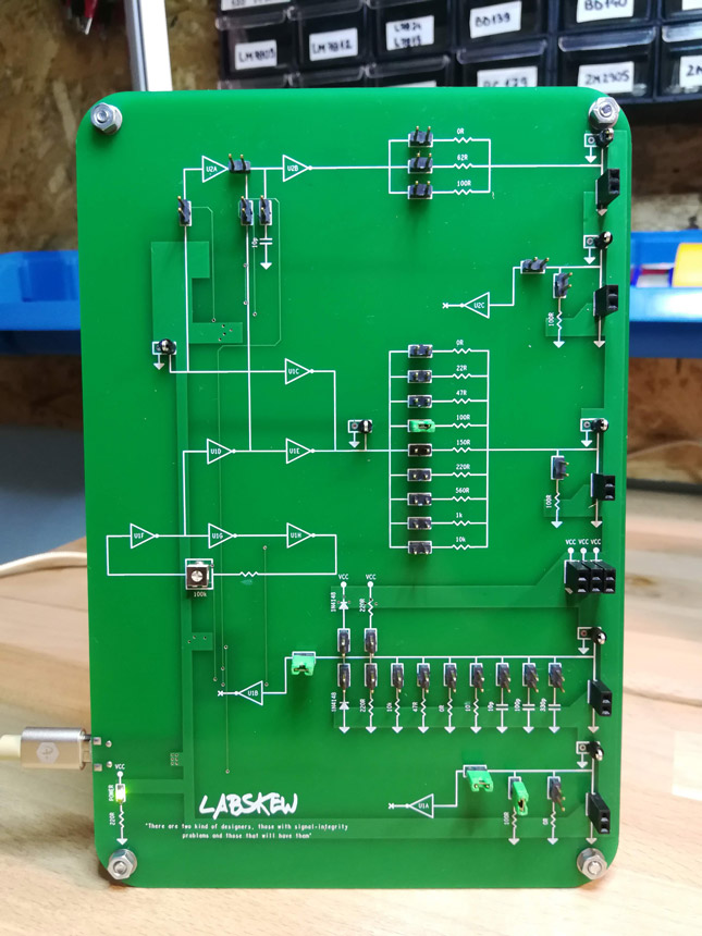 Figure 4: LABSKEW PCB platform, custom-made with jumpers placed on the TOP side
used to insert into the circuit different termination or components, a ring oscillator included
on board and only an external USB power supply required.
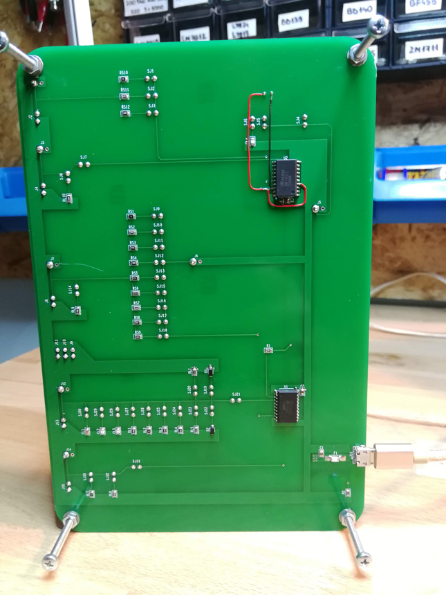 Figure 5: LABSKEW platform, TOP view. Electrical schematic embedded in the silkscreen,
power LED on the left side and test points to measure signals.
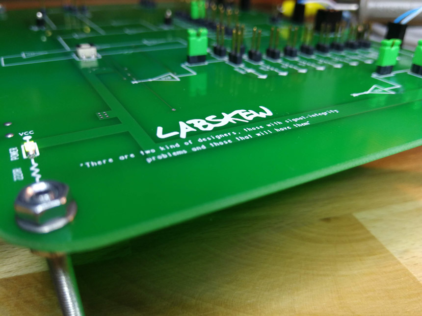 Figure 6: LABSKEW platform, BOTTOM view. All the components placed on this side,
PDN of the board well engineered to prevent signal degradation, an unfortunate mistake in
the layout was corrected with two wire jumpers.
Figure 6: LABSKEW platform, BOTTOM view. All the components placed on this side,
PDN of the board well engineered to prevent signal degradation, an unfortunate mistake in
the layout was corrected with two wire jumpers.Measurement Setup
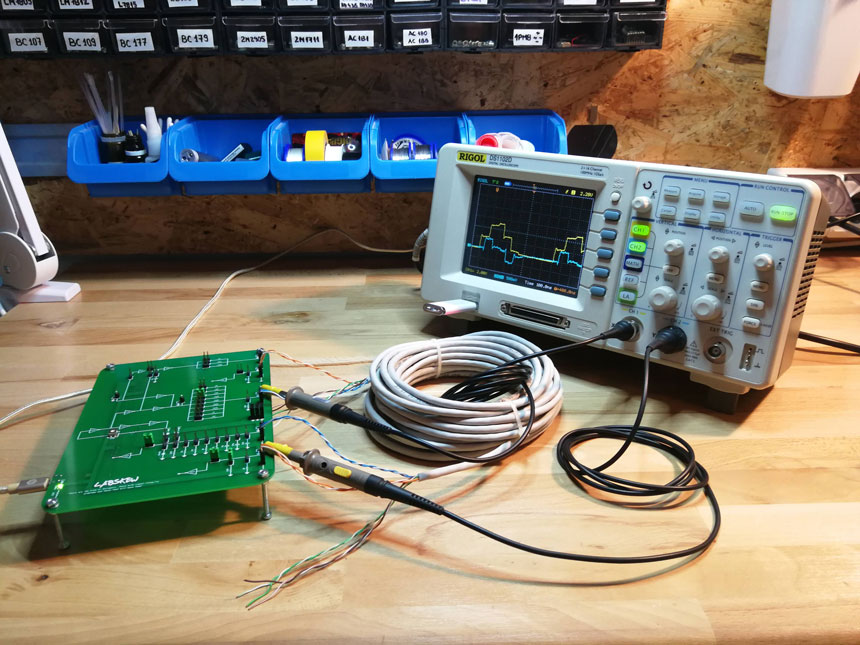 Figure 7: A 10-meters CAT5e cable is used as transmission line, one end inserted at the
oscillator and the other at some far-end terminations. Oscilloscope probes on the Near and
Far Ends of the Transmission Line.
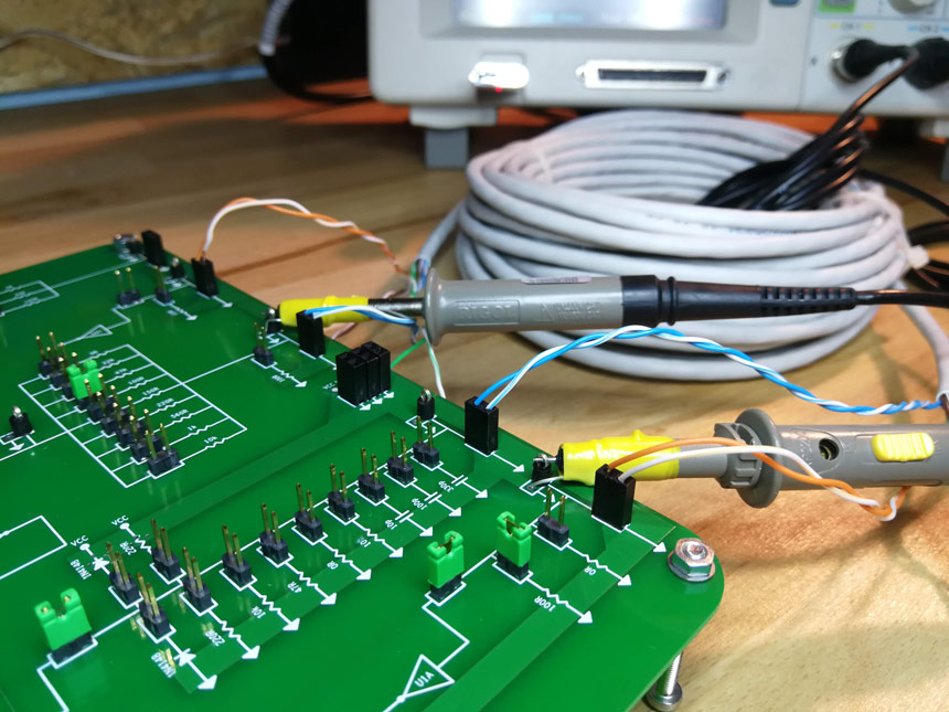 Figure 8: Oscilloscope probes engineered with 0.7mm wire warped around to serve as return
path in order to reduce their loop inductance and improve signal quality during measurements.
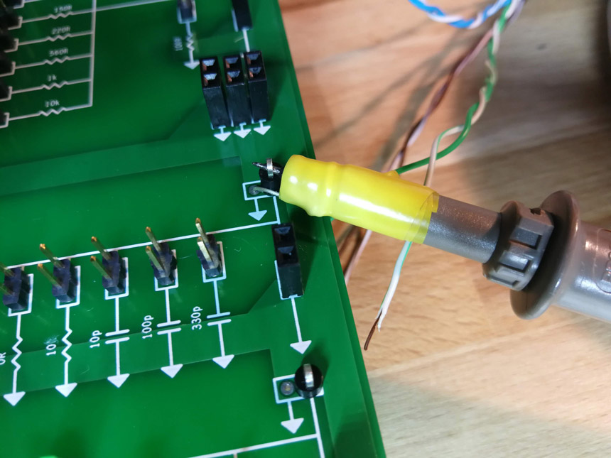 Figure 9: Measurement setup with a Rigol DS1102D Oscilloscope, LABSKEW PCB platform
and a 10-meters long CAT5e cable used as transmission line.
Figure 9: Measurement setup with a Rigol DS1102D Oscilloscope, LABSKEW PCB platform
and a 10-meters long CAT5e cable used as transmission line.Part 1: Impedance and Delays
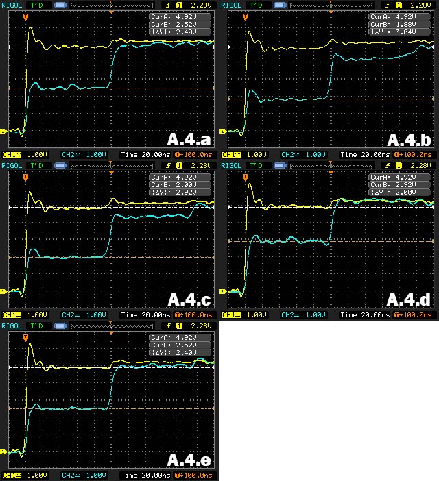 Figure 10: Transmission line with source series termination, signal before (CH1) and after
the series resistance (CH2). A.4.a: no other line is switching; A.4.b: another line without
return path is switching out of phase (odd mode); A.4.c: another line with return path is
switching out of phase (odd mode); A.4.d: another line without return path is switching in
phase (even mode); A.4.e: another line with return path is switching in phase (even mode).
Figure 10: Transmission line with source series termination, signal before (CH1) and after
the series resistance (CH2). A.4.a: no other line is switching; A.4.b: another line without
return path is switching out of phase (odd mode); A.4.c: another line with return path is
switching out of phase (odd mode); A.4.d: another line without return path is switching in
phase (even mode); A.4.e: another line with return path is switching in phase (even mode).Part 2: Reflections and Terminations
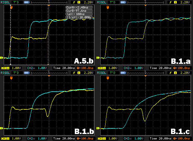 Figure 11: Transmission line with source series termination, signal at the line’s input (CH1)
and output (CH2). A.5.b: no load is connected; B.1.a: a 10pF capacitive load is connected;
B.1.b: a 100pF capacitive load is connected; B.1.c: a 330pF capacitive load is connected.
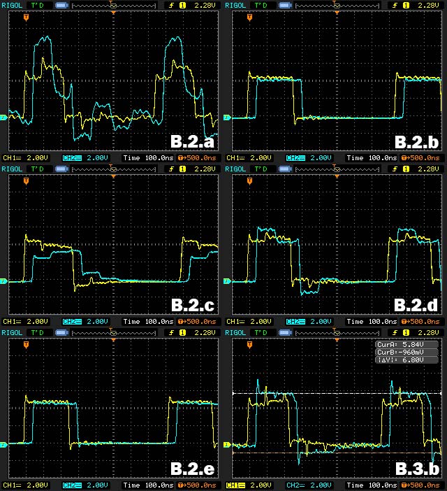 Figure 12: Effect of far-end resistor termination, signal at the line’s input (CH1) and output
(CH2). B.2.a: no termination; B.2.b: 100R resistor; B.2.c: 47R resistor; B.2.d: 220R resistor;
B.2.e: 220R resistor to GND and VCC; B.3.b: far-end diode clamp to GND and VCC;
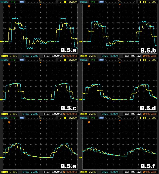 Figure 13: Effect of source series resistor termination,signal at the line’s input (CH1) and
output (CH2). B.5.a:: 22R resistor; B.5.b:: 47R resistor; B.5.c:: 100R resistor; B.5.d:: 150R
resistor; B.5.e:: 220R resistor; B.5.f:: 560R resistor.
Figure 13: Effect of source series resistor termination,signal at the line’s input (CH1) and
output (CH2). B.5.a:: 22R resistor; B.5.b:: 47R resistor; B.5.c:: 100R resistor; B.5.d:: 150R
resistor; B.5.e:: 220R resistor; B.5.f:: 560R resistor.Part 2: Cross Talk
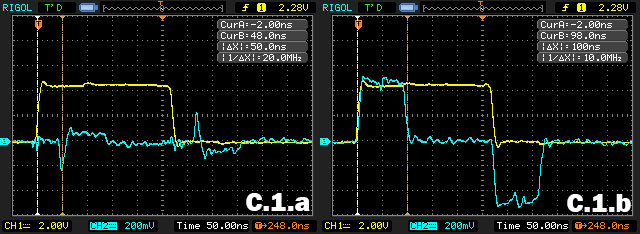 Figure 14: Aggressor transmission line terminated on 100R resistor, victim’s Near-End (NE)
and Far-End (FE) also terminated on 100R. Aggressor’s input probed with CH1 (2V/div).
C.1.a: CH2 (200mV/div) on the FE of the victim; C.1.b: CH2 (200mV/div) on the NE of the
victim.
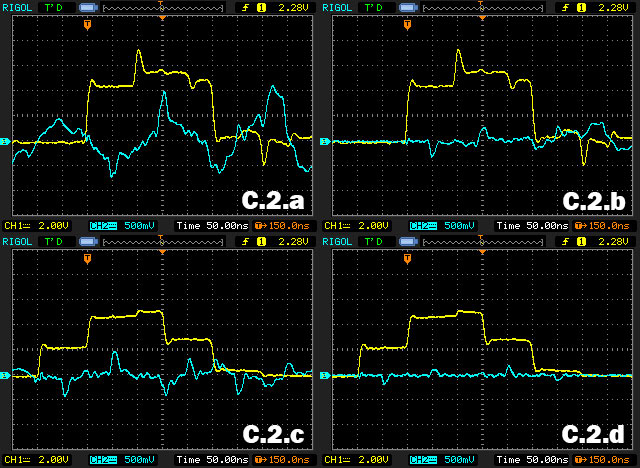 Figure 15: Termination effects on Far-End Cross Talk, signal at the aggressor line’s input
(CH1, 2V/div) and victim line’s FE (CH2, 500mV/div). C.2.a: no source series for the
aggressor, victim’s FE not terminated; C.2.b: no source series for the aggressor, victim’s FE
terminated on 100R; C.2.c: 100R source series for the aggressor, victim’s FE not terminated;
C.2.d: 100R source series for the aggressor, victim’s FE terminated on 100R.
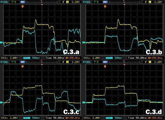 Figure 16: Termination effects on Near-End Cross Talk, signal at the aggressor line’s input
(CH1, 2V/div) and victim line’s NE (CH2, 500mV/div). C.3.a: no source series for the
aggressor, victim’s NE not terminated; C.3.b: no source series for the aggressor, victim’s NE
terminated on 100R; C.3.c: 100R source series for the aggressor, victim’s NE not terminated;
C.3.d: 100R source series for the aggressor, victim’s NE terminated on 100R.


