


Cavity resonances in two dimensions1 August 2020
Introduction
This article is the final one from a pair of three, each characterizing a different frequency interval in the impedance profile of two parallel power planes. I investigated the capacitive interval in this older article, the inductance in a blog post from the last month available here and the resonances in planes in today’s article.
I have previously stated that "every interconnect can be characterized up to a certain frequency as a lumped RLCG circuit" and the power planes are no exception. When investigating the impedance of two parallel power planes a simple series RLC circuit (or parallel if the planes are shorted) will perfectly approximate their behavior up to a certain frequency. While the ’C’ capacitance can be easily estimated with the parallel-plate approximation, the value of the ’L’ inductance depends a lot of the contact point location, as already presented in this previous post. However, above a limit frequency where the physical dimensions become comparable to the radiation wavelength, resonances will appear, points where the structures switches its behavior back and forth from capacitive to inductive. These features can no longer be captured by the simple RLC model and are only visible in a full-wave simulation.
In this article I investigate using ANSYS HFSS the wide cavities resonances and how these are influenced by the contact point location. Some resonant modes will be excited and some will not, in concordance with the contact point location. It is important to understand that resonant modes not excited by a certain contact point location are simply not visible, but they still exist as an intrinsic feature of the cavity. The element of new in this blog post is that I was also interested in correlating the simulation data with some measurements and for doing so I manufactured the same structures and measured them using an Agient 4396B Impedance Analyzer, courtesy of UPB-CETTI.
Materials and Methods
In the case of a transmission line, which is considered a one-dimensional structure, the EM waves will only propagate into one direction up and down the line’s length. The transmission line’s narrow width limits signal to propagate on the other direction, that of its width, meaning that waves can only interfere in one direction. This results in modes identified with just one index number corresponding to a half-wave multiple fitting along the long axis dimensions.
In the case of a two-dimensions cavity formed by two copper planes and a dielectric, the signal propagates differently, in both the X and Y directions and also diagonally. The principles associated with the cavity modes are identical to the one-dimensional transmission line. Waves can propagate and interfere with each other when traveling in the X direction only, in the Y direction only or with components on both the X and Y directions.
Supposing that the boundary conditions for the cavity are open at the edges so there is no phase change upon reflection, the condition for resonant peaks to build up is that an integer multiple of a half-wavelength fits between the ends of the planes. Applying this condition to waves in the X and Y directions results in two different sets of frequencies which can be further united in the formula from Equation 1. For different integer values of m and n, Equation 1 gives an estimate of all the resonant frequencies of a parallel plane structure. If m is held to 0, then the equation will only give resonant modes characteristic to the smaller dimension of the structure, noted ’l’. Bear in mind that this formula is subjected to small errors because of the dielectric constant, Dk, which varies with frequency as I previously presented in this article.
 Equation 1: Resonant modes equation
Equation 1 gives the intrinsic resonant frequencies of the cavity modes. Even if these modes can be investigated in various ways such as for example through S parameters, the one used in this investigation is the same as in previous ones, that of investigating the cavity’s input impedance. The specific resonant frequencies of each mode are intrinsic to the cavity and not affected by how or where the structure is measured. However, even if the modes exist regardless of the signal present, the efficiency of injecting a signal into a specific mode depends on how well the measurement point excites a signal. In this way, we will not be able to excite modes with half-wavelength odd numbers from the center of the cavity because they are fully suppressed.
For this investigation I designed three parallel plane structures on a 1.6mm FR4 substrate. This thickness is unusual at first and in contrast the typical dielectric thicknesses from the power integrity field. I however opted for the 1.6mm thickness because I also had to manufacture the three structures and the 1.6mm dielectric substrate along with SMA connectors fitting its size are easily available in any electronics laboratory. Even if dielectric thickness does not influence resonances in the planes as illustrated by Equation 1, it will however increase the spreading inductance as previously discussed in this blog post.
The three manufactured structures for this investigation are visible in Figure 1: a square with length (L) of 160mm, a circle with the diameter (D) of 160mm and a rectangle with length (L) of 200mm and width (l) of 90mm. Only the results for the square and the rectangle are presented in today’s article. I must mention that these dimensions were chosen only after investigating in a spreadsheet Equation 1 for different values in order to lower as much as possible the resonances below the 1.8GHz threshold (the maximum operation frequency of the Agilent 4396B used for measurements). As expected, larger planes shift the resonances toward lower frequencies.
 Figure 1: The three structures manufactured for this investigation - a square with L = 160mm,
a circle with D = 160mm and a rectangle with L= 200mm, l = 90mm. Only the square and
rectangle were investigated.
Figure 1: The three structures manufactured for this investigation - a square with L = 160mm,
a circle with D = 160mm and a rectangle with L= 200mm, l = 90mm. Only the square and
rectangle were investigated.As displayed in Figure 2, I designed contact pads for female SMA connectors in different locations of the boards. The inner pin of the SMA connector was soldered to the TOP copper layer (with clearance for the shield pads) and the shield to the BOTTOM copper layer. Investigating the structure’s impedance from its corner was expected to excite every resonant mode, probing from the middle of a margin only resonant modes with an even multiple of half a wavelength in the direction of that margin and probing from the center of the structure will excite the fewest resonant modes with even multiple of half a wavelength in both directions.
 Figure 2: Each planar structure had mounting pads for a SMA female connector in the corner,
middle of an edge and center of the board.
Figure 2: Each planar structure had mounting pads for a SMA female connector in the corner,
middle of an edge and center of the board.Measurement setup
As previously discussed, I will be investigating in this article the input impedance of the two square and rectangular structures by probing them from three different contact points situated in the corner, middle of a margin and center. I specifically designed on the physical boards mounting pads for SMA female connectors in these locations.
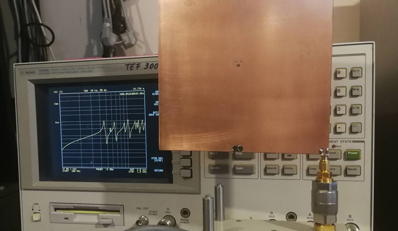
As displayed in Figure 3, I used an Agilent 4396B Network/Spectrum/Impedance Analyzer, courtesy of UPB-CETTI, for the purpose of this measurement. This device has a maximum operation frequency of only 1.8GHz, the reason why I was interested so much in engineering large structures with resonances starting at lower frequencies. Even if input impedance can be extracted from the S-parameters resulted from an 1 or 2 ports VNA measurement, I used the Agilent 43961A Impedance Test Adapter which directly measures it via an U-I method. Unfortunately, this device is only guaranteed to work up to 1GHz. However, for the pure research purpose of this investigation I pushed its limits further up to the maximum frequency of 1.8GHz available from Agilent 4396B and hoped that internal damping from reflections will not alter too much the result above the 1GHz range. As is presented in the Dissemination and Results sections, it was a decent supposition to be made.
 Figure 3: Investigated structures from this work under measurement using an Agilent 4396B
Impedance Analyzer with Agilent 43961A Impedance Test Adapter, courtesy of UPB-CETTI.
Figure 3: Investigated structures from this work under measurement using an Agilent 4396B
Impedance Analyzer with Agilent 43961A Impedance Test Adapter, courtesy of UPB-CETTI.The very important step of a high-frequency measurement is the calibration process. In this investigation I used the existing OPEN, SHORT and LOAD probes from Figure 4, part of a Type N Calibration Kit. By placing them at the output of the Impedance Test Adapter and running the ’Calibration Menu’ from the Agilent 4396B I advanced the calibration plan up to the adapter’s output. Going further, I had to custom-made three SMA terminations visible in Figure 5 to calibrate the SMA male fixture. Step-by-step I placed these fixtures at the end of the SMA connector and ran the ’Fixture Calibration Menu’ from the Agilent 4396B. This final step moved up to the SMA connector the calibration plane finally completing the pre-measurement procedures.
As far as data retrieving from the Agilent 4369B is regarded, this task was done in a rather rudimentary way via CSV files stored on a diskette (the only type of external storage supported). Furthermore, I should mention that the maximum memory size of the device was only 801 points, reason why I split the frequency interval in two: 100kHz - 100Mhz (where the structures were only capacitive and inductive) and 100Mhz - 1.8GHz (where resonances in planes were expected to take place). For each of the frequency internal I used the maximum memory available and I also repeated the whole calibration process.
 Figure 4: Calibration kit of OPEN, SHORT and LOAD part from an Agilent 85032B Type N
Calibration Kit, courtesy of UPB-CETTI.
Figure 4: Calibration kit of OPEN, SHORT and LOAD part from an Agilent 85032B Type N
Calibration Kit, courtesy of UPB-CETTI. Figure 5: Crafted calibration kit of OPEN, SHORT and LOAD with SMA female connection
type, courtesy of UPB-CETTI.
Figure 5: Crafted calibration kit of OPEN, SHORT and LOAD with SMA female connection
type, courtesy of UPB-CETTI.Simulation setup
I designed based on the physical dimensions of the three structures their 3D model in ANSYS HFSS with simulation ports placed in the corner, middle of a margin and center of the structures. Due to their large size I was forced to optimize the simulation process as much as possible. The first optimization made was to define the TOP and BOTTOM copper layers as simple sheets with a finite conductivity equal with the one of copper. Other optimization performed regards the meshing process: since the adaptive meshing that ANSYS HFSS performs would have taken a serious amount of time until the point of convergence, I constrained the meshing algorithm to generate on a specific area around the ports mesh elements with a maximum length of 3 MILs but without passing the limit of 5000 elements. This process named ’mesh seeding’ is used to improve the mesh quality and speed up simulation time.
Lastly on this topic I should mention that I performed an interpolation frequency sweep from 1 MHz to 1.8GHz for each structure to obtain the corresponding impedance profiles. In the end, I performed a discrete frequency sweep with only the resonance frequencies included when I also saved the electric fields for each point of interest.
Dissemination and results
Starting with the square cavity, in this section I present the results from simulation and measurement and how the two methods correlated. By using Equation 1 and a value of 4.65 for Dk, I calculated the resonance frequencies up to 1.8GHz (the upper measurement frequency limit of the Agilent 4396B). These values are listed as ’theoretical’ in Table 1. Bear in mind that they are prone to small errors because of the dielectric constant variation. In the following three columns from Table 1 the measured resonance frequencies are listed. Observe how probing from the corner excited all the resonant modes, probing from the middle of a margin only excited the ones with an even index in that direction and probing from the center only the ones with both indexes even.
 Table 1: Resonances frequencies for the square cavity of L = 160mm ordered from smaller
to larger values.
Table 1: Resonances frequencies for the square cavity of L = 160mm ordered from smaller
to larger values.The impedance profile for the square structure when probed from the corner is visible in Figure 6, in Figure 7 when probed from the middle of an edge and in Figure 8 when probed from the center. Results from the measurement are well correlated with the ones from the simulation even in the 1GHz to 1.8GHz range where the Impedance Test Adapter Agilent 43961A was not certified. However, results in this frequency range should not be completely trusted and small frequency shifts might appear.
Another aspect of the impedance profiles is the height of the resonant peaks which may or may not be well correlated between measurement and simulation. This heights are highly influenced by the damping provided by dielectric and conductor losses. Not accurately capturing these results may be due to the simplification made to speed up simulation time, that of using a finite conductivity sheet for the TOP and BOTTOM copper layers. One last discrepancy between simulation and measurement is the SRF (Self Resonance Point) where the structure’s behavior transitions from a capacitive one to an inductive one. This point is dependent of the spreading inductance, a measure which depends a lot of the contact point as I previously researched in this article. Due to the poor modeling of the contact point in ANSYS HFSS (only a thin rectangle was used as a port) the spreading inductance differed in simulation vs measurement which resulted in a SRF point deviation of a couple MHz.
 Figure 6: Impedance profile for the square cavity when probed from the corner, simulation
(red trace) vs measurement (green trace).
Figure 6: Impedance profile for the square cavity when probed from the corner, simulation
(red trace) vs measurement (green trace). Figure 7: Impedance profile for the square cavity when probed from the middle of an edge,
simulation (red trace) vs measurement (green trace).
Figure 7: Impedance profile for the square cavity when probed from the middle of an edge,
simulation (red trace) vs measurement (green trace). Figure 8: Impedance profile for the square cavity when probed from the center, simulation
(red trace) vs measurement (green trace).
Figure 8: Impedance profile for the square cavity when probed from the center, simulation
(red trace) vs measurement (green trace).In Figure 9a GIF animation extracted from ANSYS HFSS displays the electric field distribution along the structure for all the resonant frequencies. Needless to say that for the generation of this animation I probed the cavity from the corner and solved only at the specific resonance points the structure.
 Figure 9: Electric field lines in the square structure at the resonances frequencies, extract
from ANSYS HFSS.
Figure 9: Electric field lines in the square structure at the resonances frequencies, extract
from ANSYS HFSS.In the same manner as previously presented for the square structure, results for the rectangular one are listed in Table 2. Observe how only probing from the corner excites all the resonant modes of the structure while probing from the center only reveals the even ones. The impedance profiles resulted from the measurement and simulation are also displayed in Figures 10, 11 and 12. The same remarks above pointed are also applicable here. Last but not least, I performed a discrete sweep only with the resonance frequency to extract the GIF animation from Figure 13 where the electric field distribution in the rectangular structure can be observed.
 Table 2: Resonances frequencies for the rectangle cavity of L = 200mm and l = 90mm
ordered from smaller to larger values.
Table 2: Resonances frequencies for the rectangle cavity of L = 200mm and l = 90mm
ordered from smaller to larger values. Figure 10: Impedance profile for the rectangle cavity when probed from the corner, simulation
(red trace) vs measurement (green trace).
Figure 10: Impedance profile for the rectangle cavity when probed from the corner, simulation
(red trace) vs measurement (green trace). Figure 11: Impedance profile for the rectangle cavity when probed from the middle of its
width, simulation (red trace) vs measurement (green trace).
Figure 11: Impedance profile for the rectangle cavity when probed from the middle of its
width, simulation (red trace) vs measurement (green trace). Figure 12: Impedance profile for the rectangle cavity when probed from the center, simulation
(red trace) vs measurement (green trace).
Figure 12: Impedance profile for the rectangle cavity when probed from the center, simulation
(red trace) vs measurement (green trace). Figure 13: Electrical field lines in the rectangle structure at the resonances frequencies,
extract from ANSYS HFSS.
Figure 13: Electrical field lines in the rectangle structure at the resonances frequencies,
extract from ANSYS HFSS.Conclusion
This investigation completed along with the other two on capacitance and spreading inductance the study on power plane and their characteristics. It included simulations using ANSYS products but was however enforced by measurement of the same simulated structures using an Agilent 4396B Impedance Analyzer and an Agilent 43961A Impedance Test Adapter, both courtesy of UPB-CETTI. By placing the contact point in different key points of the structures I investigated their impedance profile and determined where the resonance points appear. Result correlated with measurement and analytical approximations to a good extend.
This investigation also has its limitation due to the ideal nature of the structures investigated, power planes rarely being in the perfect shape of a rectangle of square. Moreover, the boundary conditions are not always open and shorting VIAs or DC blocking capacitors might exist between the planes. When arbitrary shape power planes with various boundary conditions are investigated, a full-wave solver such as Ansys HFSS or Siwave should be used to determine its resonant frequencies and to investigate how the EM waves propagate along the structures.