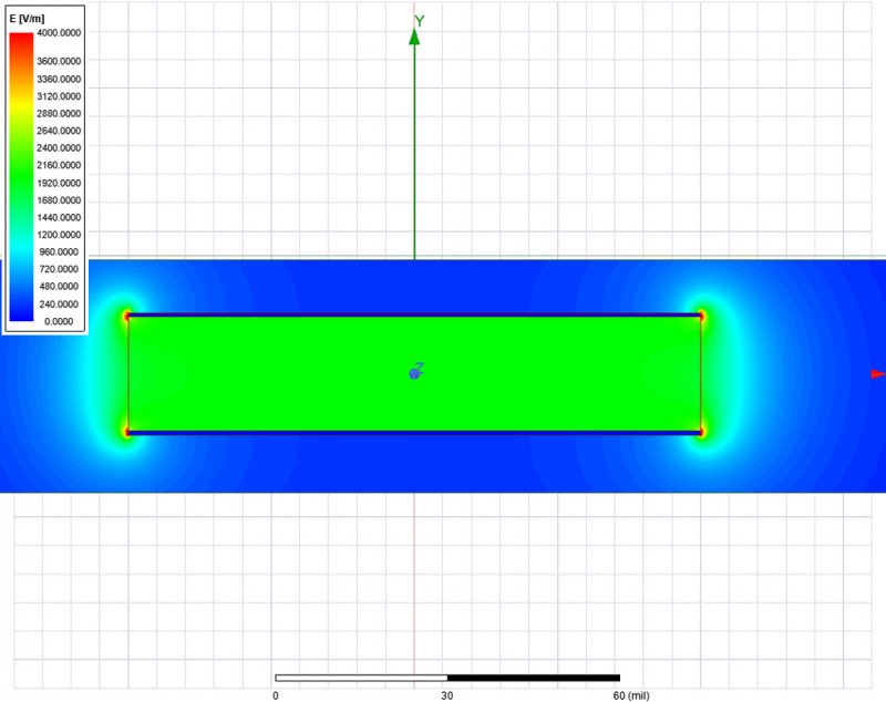
Introduction
This
article was started a long time ago and while investigating its topic of interest I stumbled
upon a different subject which quickly materialized in this
interesting study. The present
article initiates a small series of posts dedicated to investigating the limitations of different
easy and straightforward analytical approximations. For today, I directed my attention to
studying the parallel plate approximation used to calculate the capacitance between two
copper planes separated by a dielectric. This approximation does not take into account the
fringe fields at the edges of the copper electrodes, which in some cases can become a large
source of error.
Like I
mentioned in previous articles, capacitance is worth investigating since any
interconnect from the signal and power integrity field can be characterized as a simple RLCG
model at least as a first order model. Certain formulas exist and help to the characterization
of different circuit elements but as any approximation, these also have limitations. If you
do not want to go beyond the fence, you have to know where the fence is situated. In other
words, it is important to understand these limitations in order to avoid possible errors.
In
this article I evaluate different aspect ratios Width/Height (W/H) capacitive structures
to determine the limitations of the parallel plate approximation. Cases where the dielectric
extends beyond the edges of the copper planes named power puddles are also studied. In
the end, once the capacitance addition caused by the fringing effect is determined, I use
the corrected parallel plate formula to calculate the capacitance of a small 3D capacitive
structure and I match the analytical results with simulation data.
Materials and Methods
The capacitance between two parallel plates can be calculated using Equation 1, were W,
H and Len are the width, height and length of the structure as displayed in Figure 1 and
ε0 is the vacuum permittivity equal to 0.225 pF/inch. εr is the
electrical relative permittivity
referred as Dk in this work and is equal to 1 for vacuum and 4.4 for FR4 epoxy. However,
Dk varies slightly with frequency due to dipole orientation effects as discussed in a
previous
blog article,
Frequency-Domain characterization of FR-4 dielectric using Djordjevic-
Sarkar algorithm. If the capacitance per unit length is required, Equation 2 which resulted
by dividing the expression from Equation 1 with the length of the structure is used. In this
current investigation, unless otherwise mentioned, all the capacitance values are given per
unit length (even if the subscription from Clen is omitted).
 Equation 1:
Parallel plate approximation
 Equation 2:
Parallel plate approximation per unit length
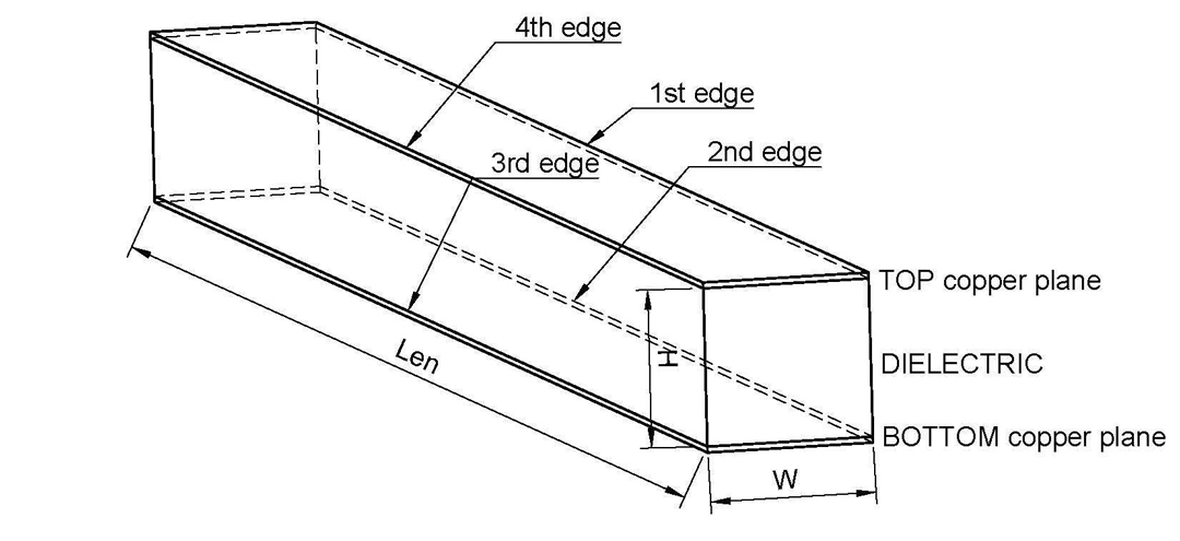
Figure 1: Structure of a parallel plate capacitor, with two copper electrodes separated by a
dielectric. Results in this investigation are given per unit length, unless otherwise mentioned.
Moreover, fringe field capacitance is given per unit length per individual edge of conductor.
The formulas from Equations 1 and 2 do not take into account the fringe field
lines from
the edges of the two copper planes. In other words, the electric field lines close between
the generically named TOP and BOTTOM plates through the dielectric material but also
escape the area in the proximity of the edges, closing through air, vacuum of whatever the
type of the environment is. If the fringe field contribution is small with regard to the total
capacitance of the planes, this addition becomes insignificant.
In this article we investigate how large a capacitive structure must be in order for the
fringe field contribution to become negligible. The structures investigated are parallel plate
capacitors simplified to a 2D geometry of a transversal plane sectioning the complete structure.
Since only 2D structures are investigated, all the results are given per unit length. It was
observed that if the structure is large enough with a high W/H, the capacitance contribution
of the fringe field saturates to a constant value. This contribution called Clen-fringe is also in
this work given per unit length and is furthermore expressed per edge of conductor. In other
words, for the structure from Figure 1 the total corrected capacitance can be calculated using
Equation 3.
 Equation 3:
Total capacitance per unit length
The error of using the parallel plate approximation is calculated by dividing the fringe
field contribution to the total capacitance of a structure, as is numerically expressed in
Equation 4. The error results are as usual presented in percents.
 Equation 4:
Error of using parallel plate approximation
Lastly, the material through which the fringe field lines close is also of interest. In the
case of parallel plate structures such as the case from Figure 1, this material is nothing more
than air or vacuum (in rare and special occasions such as the case of a board immersed in
water this material could differ from air). However, usually found in practical applications
are not the above described structures but the ones in which the dielectric extends far beyond
the edges of the copper planes. This is the case of islands from power planes located on two
different layers of a circuit board, reason why this structures are also called power puddles.
In this work I investigate both parallel planes and power puddles, with some interesting
variations resulting in the end for both of these structures.
Simulation setup
A
simulation tool as ANSYS 2D Extractor provides the capacitance of a structure while also
including all the second-order effects such as fringing fields. In this way, the results from
the simulation tool are considered in this investigation as total capacitance with the fringing
effect also included while the parallel plate approximation includes only the capacitance of
the planes. Since the geometry was simplified to a 2D plane resulted by sectioning the 3D
geometry with a transversal plane, ANSYS 2D Extractor was suited for this investigation.
I studied in this article both parallel plate structures (Figure 2 right side) and also power
puddles (Figure 2 left side). While investigated parallel plate structures I extracted results for
both the case when plates are filled with air (Dk = 1) and also with FR4 epoxy (Dk = 4.4). In
the case of power puddle structures I only considered the case of a FR4 epoxy dielectric fill.
Simplifying the geometry to a 2D transversal section provided an extremely reduced and
high accuracy simulation.
The structures from Figure 2 were parameterized with the Height (H) and Width(W)
available for various sweeps. By keeping the H to a fixed 20 MILs value and varying the W
from 5 to 600 (aspect ratios from 0.25 to 30) a total of 45 simulation points were obtained
for each of the three cases: parallel plates with air or FR4 dielectric and power puddle with
FR4 dielectric. ANSYS 2D Extractor provided the results exactly in the way needed for this
investigation, as RLCG per unit length.
 Figure
2: Parameterized geometries used in this investigation. From left to right, the one
used for power puddles and the one used for parallel plate.
As mentioned in the Introduction, the Dk of a dielectric material is not perfectly constant
and actually varies slightly with the increase of frequency. In this investigation, causal
materials are disabled, meaning that ANSYS 2D Extractor and HFSS do not implement the
Djordjevic-Sarkar algorithm for the Dk of the materials involved. I opted for this setting
which is in no case practical for real simulations to force the software tools to consider a
precisely fixed Dk of 4.4 for the FR4 epoxy regardless of frequency. If you are interested
how a frequency dependence dielectric constant should be set in ANSYS material libraries,
check out this previous article where I broadly discuss this topic.
Because causal materials were disabled in this specific investigation, the frequency
where the capacitance extraction was performed in ANSYS 2D Extractor is not of interest.
Extracting it at 100 kHz or 100 MHz would have provided the same capacitance results. I
should mention also that ANSYS 2D Extractor is only a quasi-static field solver, limitation
which raised no issues in this specific study where transmission line effects were not of
interest.
For high aspect ratios, the fringe capacitance was observed to stabilize at a fixed value.
For both types of structures I was also interested in the error committed when using only the
parallel plate formula. In this way, by using Equation 4 for high aspect ratios above the point
where Clen-fringe becomes constant, I obtained the error possibly committed by not taking
into account the fringe field contribution.
In the end, I also simulated a full 3D structure of 200·20·1000 MIL visible in Figure
3 in
ANSYS HFSS. I obtained the total capacitance of the structure using Equation 3. The result
from the corrected approximation perfectly matched the impedance profile of the structure
provided by the simulator validating once again the findings of this work.
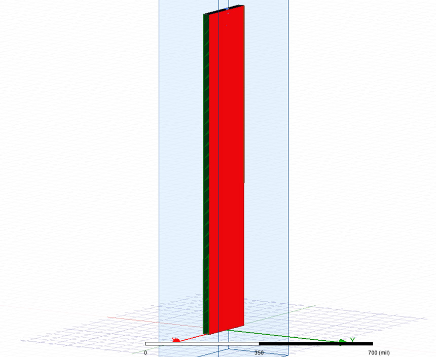 Figure 3:
Small parallel plate capacitive structure with fixed 200·20·1000 MILs dimensions.
3D Design simulated in ANSYS HFSS to investigate the effect of fringe fields.
Dissemination and results
I
mention that there is no tabulated data included in this part of the article due to the large
size of the dataset. However, all the important results are displayed in the form of graphs in
this section and further discussed. I start the dissemination and results part with the parallel
plate structure. This geometry was investigated in two cases: the planes filled with air (Dk =
1) and with FR4 epoxy (DK = 4.4). Height was kept to a fixed value of 20 MILs and width
was varied from 5 to 600 MILs (aspect ratios from 0.25 to 30).
The Clen-fringe was extracted by subtracting from the value provided by the simulator the
one from Equation 2 corresponding to the parallel plate approximation. The result was once
again divided by 4 to obtain a value per edge of conductor. The variation of Clen-fringe with
the aspect ratio is provided in Figure 4 for Dk = 1 and in Figure 5 for Dk = 4.4.
Note that
there is almost no difference between these two graphs since they both describe the fringe
fields through the same environment material, the air surrounding this structure.
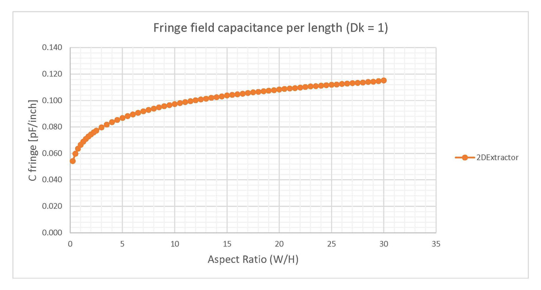 Figure 4: Fringe field capacitance of parallel
plates when the dielectric is vacuum (Dk = 1).
Results are given per length per edge of conductor.
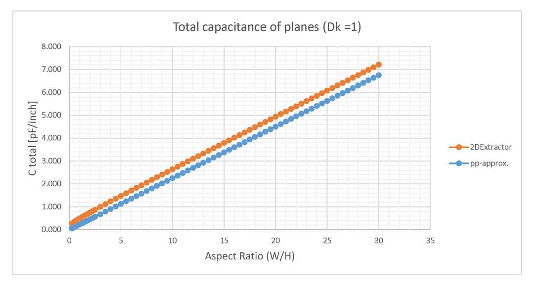 Figure 5: Fringe field capacitance of parallel
plates when the dielectric is FR4 epoxy (Dk =
4.4). Results are given per length per edge of conductor.
In Figures 6 and 7 the capacitance of planes is plotted for the same parallel
plate structures
in the case of air dielectric fill or FR4 epoxy. These graphs include both results from 2D
Extractor and also from the parallel plate approximation. In the case of plates filled with
air, the difference between the parallel plate approximation and the 2D Extractor is higher
than in the case of plates filled with FR4 epoxy, which generates a higher error in the first
case. However, the capacitance addition caused by the fringe fields is the same for both of
these cases. These previous observations are explained by the fact that in the case of FR4
epoxy the capacitance located inside the parallel plates captured by the approximation from
Equation 2 is significantly higher than the fringe field addition.
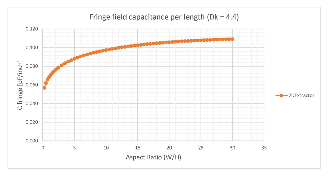 Figure 6: Total capacitance for parallel planes,
comparison between the parallel plate approximation
and 2DExtractor (Dk = 1).
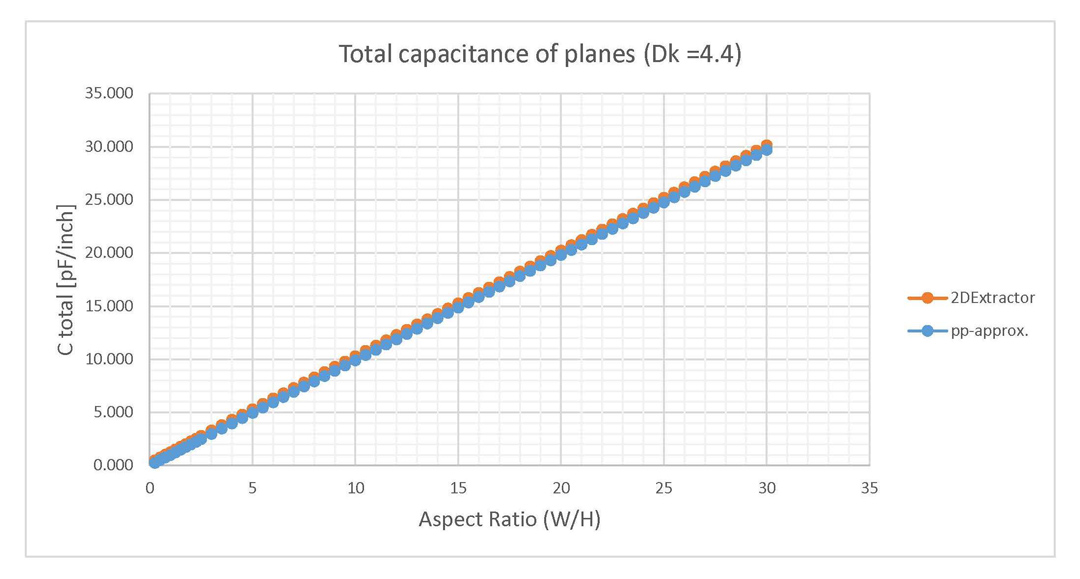 Figure 7: Total capacitance for parallel planes,
comparison between the parallel plate approximation
and 2DExtractor (Dk = 4.4). Difference of values is smaller than in the case of Dk = 1.
The most important result from the investigation so far is that the fringe capacitance
saturates to a fixed value around 0.11 pF/inch per edge of conductor for parallel plate
structures situated in air. This result is independent of the dielectric height, the only condition
being the aspect ratio to be higher than 10. This assumption is verified by performing a
variation of 20 values for W and H, all with the aspect ratio held constant to 10. The results
from Figure 8 validated this assumption, with the fringe capacitance constantly situated
around 0.10 pF/inch per edge of conductor for any W and H value as long as their ratio was
fixed to 10.
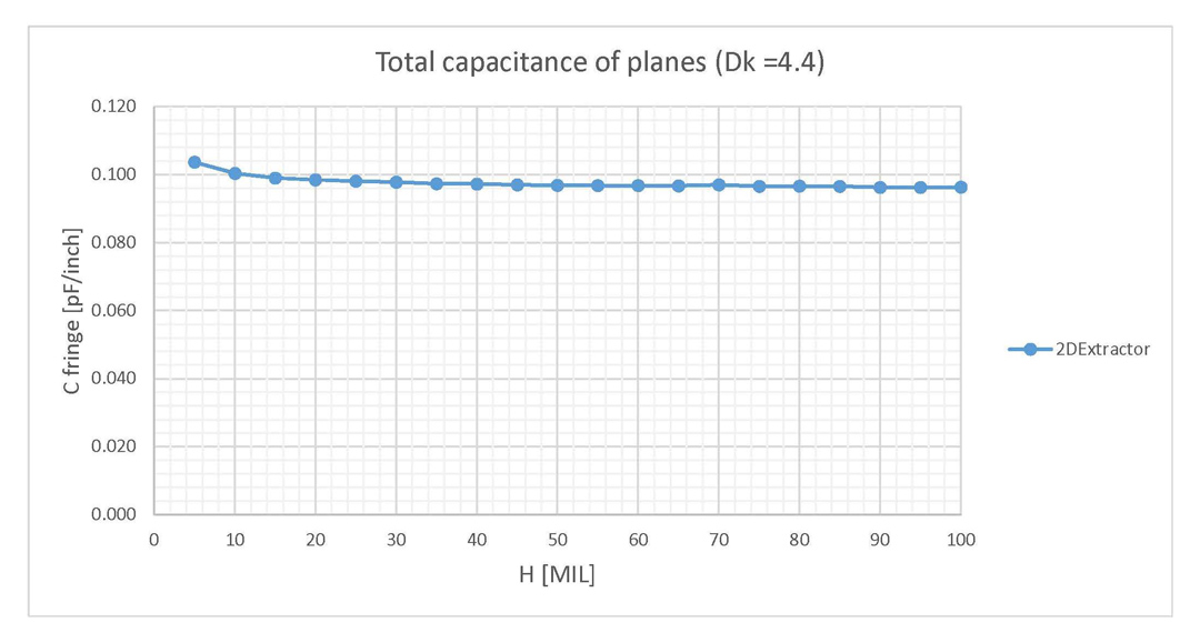 Figure 8: Total capacitance for parallel planes when height H is
varied from 5 to 100 but the
aspect ratio W/H is fixed to 10. Results are given per length per edge of conductor.
For the parallel planes structures I also investigated the error committed by using only the
approximation from Equation 2 and not taking into account the fringe field effect. Already
observed in Figures 6 and 7 and briefly discussed above, this error is now plotted
in Figure 9.
As you can see, only aspect ratios higher than 10, the point where Clen-fringe saturates to a
fixed value were used in this sweep.
Notice from Figure 9 that the error is lower for plates filled with air as compared to the
ones filled with FR4 epoxy. For an aspect ratio of 10, this error is 20% in the case of air
and drops to 5% for FR4 epoxy. This error graph is a good figure of interest when using the
parallel plate approximation to investigate the capacitance between two parallel planes.
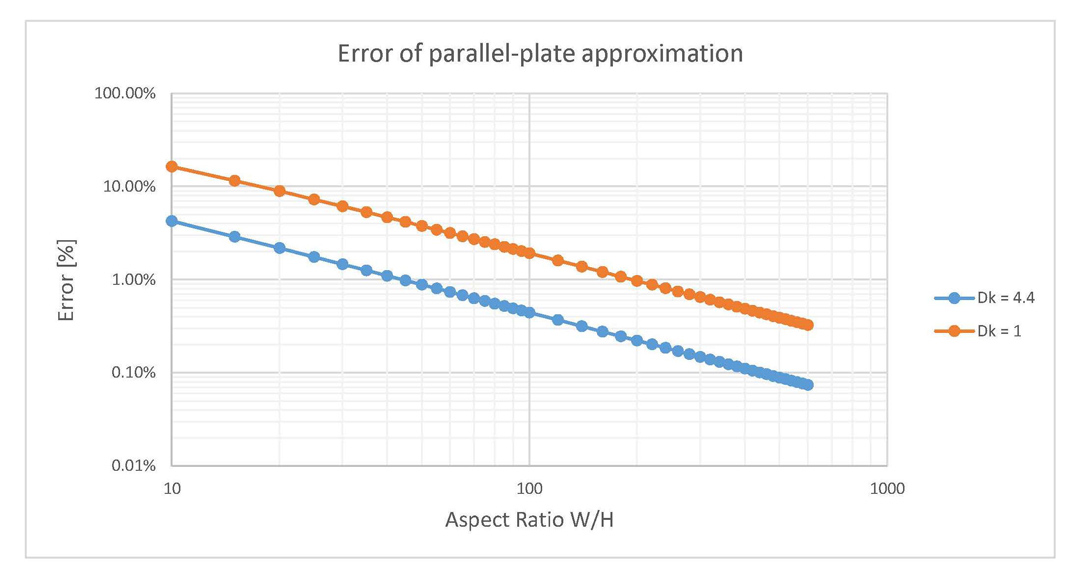 Figure 9: Error of parallel plate approximation for
parallel plane structures when the dielectric
is vacuum (Dk = 1) and FR4 epoxy (Dk = 4.4).
Secondly, I also investigated the power puddle structures from the left side of Figure 2,
where only a FR4 epoxy fill was of interest. I mention that this type of structures is what you
would usually encounter in a circuit board and results from two partial power and ground
planes, hence its name. The same height of 20 MILs and variations of width from 5 to 600
MILs (aspect ratios from 0.25 to 30) were also used and the fringe field capacitance from
Figure 10 resulted through the same methods already discussed. Observe that this time the
fringe field capacitance is higher, settling around the value of 0.20 pF/inch of conductor edge
for aspect ratios higher than 10. This increase in the fringe capacitance was expected due to
the fact that now the fringe field lines are closing through the FR4 dielectric material.
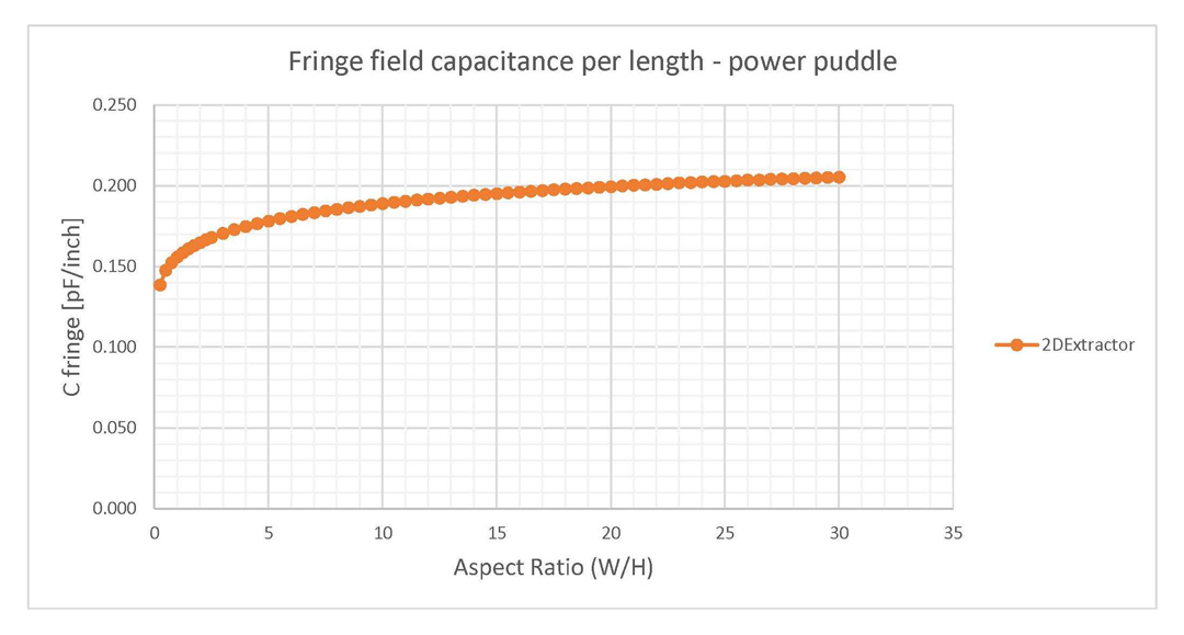 Figure 10: Fringe field capacitance of power
puddles. Results are given per length per edge
of conductor.
The error of using only the parallel plate approximation for power puddles was also
investigated using Equation 4 and results are displayed in Figure 11. Since the
fringe field
capacitance in this case is higher than in the case of parallel plane structures, the error is also
higher. For the same aspect ratio of 10 is observed that now the error is around 9% while
previously was only 5%.
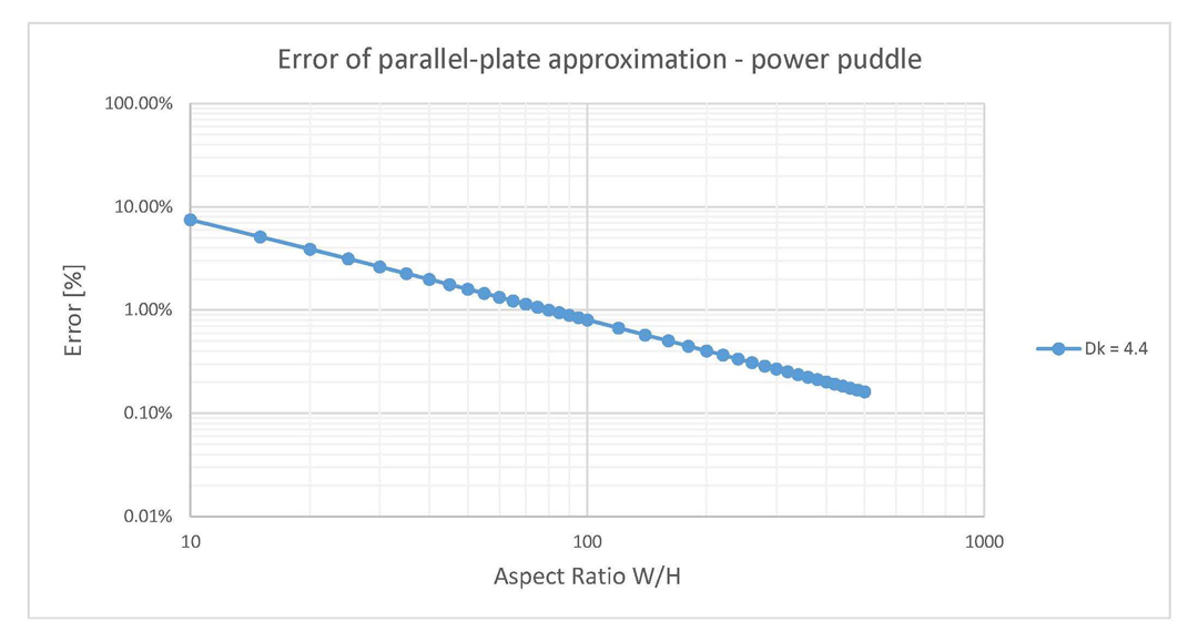 Figure 11: Error of parallel plate approximation for
power puddle structures. The dielectric
is FR4 epoxy (Dk = 4.4).
This error graph is also a good figure of interest when using the parallel plate approximation
to investigate the capacitance of power puddles. Observe that to obtain a lower than 1%
error, an aspect ratio above 100 is required. It might seem a lot at first, but usually power
planes have a 10 MILs separation dielectric or even lower. This value leads to a 1000 MILs
width which is usually found on a regular circuit board.
With all the variations performed we obtained a fringe field addition value saturated to
0.11 pF/inch of conductor edge for parallel plate structures. I investigated one capacitive
structure of this type with dimensions of 200·20·1000 MILs using ANSYS HFSS. With an aspect
ratio W/H = 200/20 = 10, the structure can be considered to have a constant Clen-fringe =
0.11 pF/inch of conductor edge. Using Equation 3 and the parallel plate approximation I
obtained a Clen-total = 10.34 pF/inch which results in a capacitance of 10.34 pF for an 1-inch
long structure. The impedance profile extracted from Z11 displayed in Figure 12 has the
impedance of a 10.34 pF capacitor imposed to the graph. Observe how this structure can
be perfectly approximated with a capacitor up to 0.3 GHz, a frequency corresponding to
the length of 1000 MILs being equal to λ/10. In the next frequency interval from 1.5 GHz
to 3 GHz the structure becomes inductive and then has a transmission line behavior, some
interesting topics for future blog posts.
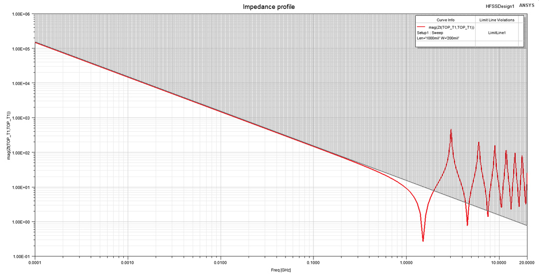 Figure
12: Impedance profile from Z11 of 3D capacitive structure from Figure 3. In can be
approximated with a 10.34 pF capacitor to the frequency of 0.3 GHz.
Conclusion
In this article I investigated the parallel plate approximation used to calculate the capacitance
between two copper planes separated by a dielectric. This approximation does not take into
account the fringe fields at the edges of the copper electrodes, which in some cases can
become a large source of error leading to some limitations. Dielectric materials usually have
a slightly frequency dependent dielectric constant which is implemented in ANSYS products
by using the Djordjevic-Sarkar algorithm, more about this discussed in a previous article
here. However, in this specific investigation I ignored any frequency dependence to easily
compare simulation results with the analytical approximation.
ANSYS 2D Extractor was used to extract the total capacitance between two parallel
planes which of course also included the fringing effect. By subtracting from this value the
result from the parallel plate approximation, the fringe field capacitance was obtained. All the
results were given in a form per unit length per edge of conductor. Simulations have shown
that the fringe field capacitance is 0.20 pF/inch of conductor edge in the case of dielectric fill
extending beyond the edge of the copper plane or only 0.11 pF/inch of conductor edge when
the dielectric fill stops at the margin of the plane. These fixed values are only valid for higher
aspect ratios W/H above the threshold of 10.
Lastly, the error of using the parallel plates approximation was calculated and was found
that for high aspect ratios it becomes considerably smaller. This conclusions give important
insight into the limitations of using the parallel plates formula and offer a quantitative
approach to correct its results if needed by adding the fringe capacitance to its result.
Finally, analytical approximations are extremely useful and knowing their exact limitations
is absolutely mandatory since this can make the difference between a good design and a
marginal one.
References
[1] Larry D. Smith, Eric Bogatin. Principles of Power Integrity for PDN Design – SIMPLIFIED.
Prentice Hall, 2017. ISBN 978-0-13-273555-1.
[2] S. C. Thierauf, High-Speed Circuit Board Signal Integrity. USA: Artech House, Inc.,
2004. Propagation of Electric Fields in Exposed Microstrip. pp. 195–196.


