

How to Use Trace Reinforcements to Optimize PCB Models14 January 2021
Ora: 18:00 (Romania)
The increasing complexity of 21st century electronics continues to drive demand for comprehensive multiphysics simulations. Simulation helps engineers determine potential failure risks before physical prototyping, making it one of the most beneficial and cost-effective solutions for electronics manufacturers. However, there are often significant modeling challenges associated with the increased layout complexity of printed circuit boards (PCBs), including finer density traces and intricate routing structures.
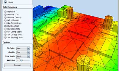
Fortunately, there are a number of modeling techniques that exist that allow for more complex and accurate PCB models. These techniques range from homogeneous effective material properties to trace mapping to detailed trace modeling. In this webinar we will focus on a trace modeling technique called trace reinforcements.
In the trace reinforcement method, copper traces are modeled with 1D or 2D elements that are embedded within 3D structural elements. This strategy allows for the inclusion of detailed trace geometry features in a highly complex PCB model without the unreasonable body/element counts that come with a standard 3D body trace modeling approach.
This webinar will discuss when to use trace reinforcement modeling, the accuracy and efficiency the methodology offers, and how to use Ansys Sherlock to automate the creation of a trace reinforcement model.